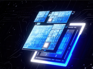
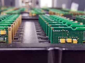
The rapid development of artificial intelligence is quietly driving the transformation of a traditional industry: the PCB (Printed Circuit Board) is no longer just a simple electronic connector but has become key to unleashing AI computing power.
Driven by demands from AI servers, high-speed communication, and automotive electronics, PCB technology is undergoing a comprehensive upgrade across three major dimensions: materials, processes, and architecture.
As AI models become increasingly complex, the hardware infrastructure supporting these models must evolve accordingly. In this technological revolution, the PCB industry is welcoming a brand new "golden age."
01 AI Computing Power Drives Explosive Growth in the PCB Market
The rapid development of AI is reshaping the PCB industry's market landscape. According to CICC research reports, the AI PCB market size is expected to reach $5.6 billion by 2025, and will further grow to $10 billion in 2026, showing explosive growth.
Prismark predicts that the global PCB output value will reach $94.661 billion by 2029, with a compound annual growth rate (CAGR) of 5.2% from 2024 to 2029.
This growth is primarily driven by the server/storage sector, which is expected to have a CAGR of 11.6%, significantly higher than other application areas.
Since 2006, Mainland China has surpassed Japan to become the world's largest PCB production base. In 2024, the PCB output value in Mainland China was $41.213 billion, accounting for 56% of the global total.
It is projected that by 2029, the PCB output value in Mainland China will reach $49.704 billion.
02 The Revolutionary Impact of AI on PCB Technology
High-Layer Count and High-Density Interconnection
The technical requirements for PCBs in AI servers are far higher than those for traditional products, achieving a true "increase in both volume and price." Generally, AI server PCBs typically contain 20 to 28 layer multilayer structures, far exceeding the 12 to 16 layers of traditional servers.
In terms of price, the value of PCBs used in AI servers is several times that of traditional servers, with a single-unit PCB value reaching $8000~$10000.
Material Upgrades: Born for Speed
Due to the "skin effect," if conventional copper foil continues to be used in high-speed PCBs, signal "distortion" becomes increasingly severe as the signal transmission frequency increases.
Therefore, the application of low-roughness copper foil is becoming more and more widespread in current high-speed materials.
To achieve high frequency and high speed in PCBs, improvements to the resin, glass fiber, and overall structure are also necessary. High-end materials such as M9/PTFE resin, HVLP copper foil with Rz≤0.4μm, and low-loss quartz cloth have become key to achieving 224G high-speed transmission.
In the Rubin platform, to achieve low loss and low latency, material usage has been comprehensively upgraded, including the Switch Tray adopting M8U grade and 24-layer HDI board design, while the Midplane and CX9/CPX introduce M9, with the highest layer count reaching 104 layers.
Process Innovation: Towards a Finer World
On the process side, mSAP/SAP processes are pushing line width/space below 10 micrometers, with laser drilling, back drilling, and high multilayer stacking processes supporting high-density interconnection.
A revolutionary change is also happening on the architecture end. CoWoP packaging connects the chip directly to the PCB by removing the ABF substrate, placing extremely high demands on board surface flatness, dimensional stability, and manufacturing yield.
Orthogonal backplane solutions need to use low-loss materials like M9 or PTFE to meet the requirements of 224G SerDes transmission.
03 How AI is Changing the PCB Design and Manufacturing Process
Innovation in Simulation Technology
Facing the challenges of high-frequency design, leading companies in the industry are developing advanced simulation technologies. OKI Circuit Technology recently developed high-frequency via simulation technology for 1.6 Tbps class high-speed transmission PCBs.
In frequency bands exceeding 50 GHz, traditional modeling methods struggle to accurately represent the effects of the manufacturing process and material properties in high-frequency regions. OKI's new technology integrates high-precision manufacturing data, 3D electromagnetic field analysis, and production-optimized design, allowing engineers to predict actual via performance before manufacturing.
AI-Powered Design Tools
Siemens' Digital Industries Software division announced at the 2025 Design Automation Conference the launch of an AI-enhanced toolset suitable for EDA design flows.
This dedicated EDA AI system provides secure, advanced generative and agent-based AI capabilities, offers unparalleled customization features, and enables seamless integration throughout the EDA workflow.
Aprisa AI software supports next-generation AI features and methodologies from RTL to GDS. Its functions include AI design exploration, which can adaptively optimize Power/Performance/Area for a given design.
04 The New Landscape of Supply Chain and Capacity
Wave of Capacity Expansion
Driven by AI demand, leading PCB companies like Shenghong Technology, Wus Printed Circuit, and Avary Holding are actively expanding production, creating a resonance between material upgrades and capacity expansion.
According to CITIC Securities estimates, leading Chinese PCB companies will form project investments totaling 41.9 billion yuan in 2025-2026.
In terms of capacity, major manufacturers are actively making plans—Shengyi Electronics' Thailand base and domestic intelligent computing center project are accelerating construction; Kingboard's 5 billion yuan investment in Zhuhai will add 800,000 square meters of HDI capacity, expected to start production in 2026; Wus Printed Circuit is also actively promoting a total investment of 4.3 billion yuan in high-end PCB projects and customer certification and import for its Thailand base.
Beneficiaries in the Equipment and Material Supply Chain
AI is driving the industry towards higher layer counts, finer wiring, and higher reliability, placing higher demands on processing technology. Drilling, exposure, plating, and inspection, as core links in PCB production, directly determine the interconnection density, signal integrity, and production yield of circuit boards.
AI servers demand higher volume, density, and performance from PCBs, corresponding to higher requirements for equipment precision and faster depreciation. Links such as exposure, drilling, plating, and inspection benefit the most.
Domestic PCB equipment manufacturers are expected to seize the opportunity presented by the AI PCB boom window, accelerate the verification of emerging technologies, actively meet incremental demand, and achieve expanded domestic market share and increased value.
In the upstream materials sector, copper foil is upgrading from HVLP1 to HVLP5, electronic cloth is iterating towards the third generation of low dielectric cloth, and resin is upgrading towards hydrocarbon and PTFE.
05 Future Trends: PCB's Position as the Computing Core is Consolidated
According to TrendForce research, AI server design is undergoing a structural transformation, from the cable-less architecture of the NVIDIA Rubin platform to the high-layer HDI design of self-developed ASIC servers by cloud majors. PCBs are no longer just circuit carriers but have become the core for releasing computing power.
The cable-less interconnect design adopted by the Rubin generation servers is the starting point for the reversal of the PCB industry's status. In the past, high-speed transmission between GPUs and Switches relied on cables, but now it is directly undertaken by multilayer PCB boards such as Switch tray, Midplane, and CX9/CPX, making signal integrity and transmission stability the core indicators of design.
This transformation increases the PCB value per server by more than twofold compared to the previous generation.
TrendForce believes that 2026 will be the new starting point for PCBs driven by "technology content driving value." As AI models become increasingly complex, the hardware infrastructure supporting these models must correspondingly develop. The position of PCB as the core of computing power will continue to be consolidated.
We are witnessing the technological rebirth of a traditional industry. PCB has leapt from an obscure circuit carrier to a core component of AI computing power infrastructure. With the continuous growth in demand from AI servers, high-speed communication, and automotive electronics, the PCB industry is ushering in an era of high frequency, high power, and high density.
Future PCBs will not merely be carriers for connecting components but will be a key factor determining system performance. Driven by AI, the PCB industry is undergoing a profound qualitative change, a transformation that will reshape the landscape of the entire electronics industry.


